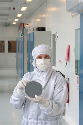
VTT method accelerates the development of microelectronics in three dimensions

VTT Technical Research Centre of Finland has developed the unique PillarHall test structures to accelerate the market entry of three-dimensional, small, efficient and low-power but high-performance electronic components. This will benefit developers of challenging thin film and related manufacturing processes, and thereby the entire electronics industry value network.
There has been occasional speculation on whether Moore’s Law remains valid. Transistors are already being packed into squares so small that their rate of shrinkage is accelerating in three dimensions. For example, the equivalent of 4 billion 72-storied skyscrapers on a dime has enabled the creation of a 256 GB memory chip.
VTT has developed record-high aspect ratios on an extremely challenging scale (10,000:1 and 100 nm) for the 3D test structures on silicon chips and wafers, to meet the requirements of the most challenging applications. Such applications include in addition to semiconductor circuits, also optics, MEMS, sensors, thin film batteries and photovoltaics.
“What makes our chips special is that we have turned the analysis 90 degrees and adopted a lateral rather than the traditional vertical approach, which enables much faster data production and lead times than current methods. For example, cross-sectional analysis of microscopic vertical structures can take weeks, whereas Pillar Hall provides data without delay. Other advantages include accuracy, versatility and compatibility with varying process conditions,” says inventor and Senior Scientist Riikka Puurunen (D.Sc. (Tech.)) of VTT.
The PillarHall test structure also introduces a new parameter space into the analysis, which allows more efficient thin-film R&D, adoption of new industrial applications and process control.
PillarHall is being funded under Tekes’ Research Commercialisation Programme. This involves developing silicon chips for quantifying thin-film conformality, which is a key value proposition of ALD (Atomic Layer Deposition) technology. ALD has originally been developed in Finland and Finland’s key ALD technology players are involved in the Project Advisory Group: ASM, Beneq, Picosun, the University of Helsinki and Okmetic Oy.
VTT is currently working with PillarHall’s 3rd-generation prototypes, which have been successfully tested by Finnish partners and a number of research institutes. VTT is now seeking international partners, in particular, as test users to push forward with the testing and commercialisation of the chips.
”The interest shown by industry and the positive experiences of users build confidence in our vision that PillarHall chips and wafers could one day become the conformality standard and be commercially available,” says Project Manager Mikko Utriainen (D.Sc. (Tech.).
More information about the project:
http://pillarhall.com
VTT Blog: Moore’s law - is it a spring of productivity? https://vttblog.com/2017/05/30/moores-law-is-it-a-spring-of-productivity/
Further information:
VTT
Mikko Utriainen, Project Manager
tel. +358 40 753 7415
mikko.utriainen@vtt.fi
Further information on VTT:
Milka Lahnalammi-Vesivalo
Communications Manager
+358 40 5457 828
milka.lahnalammi-vesivalo@vtt.fi
www.vtt.fi
VTT Technical Research Centre of Finland Ltd is the leading research and technology company in the Nordic countries. We use our research and knowledge to provide expert services for our domestic and international customers and partners, and for both private and public sectors. We use 4,000,000 hours of brainpower a year to develop new technological solutions. VTT in social media: Twitter @VTTFinland, Facebook, LinkedIn, YouTube, Instagram and Periscope.
Tags:


